The Field-Programmable Gate Array (FPGA) has made a splash in the traditional communications and integrated circuit (IC) design domains with its parallel hardware acceleration capability and programmability. After decades of development, the FPGA is no longer an emerging hardware device. However, the FPGA has never been widely promoted to ordinary users because of its high development threshold and high release and deployment protection requirements of hardware acceleration algorithms. Consequently, the computing potential of the FPGA has not been fully utilized.
Alibaba Cloud virtualization platform's heterogeneous computing and high-performance computing teams have long been committed to popularizing computing resources. The high-performance computing team is developing Elastic High Performance Computing (E-HPC) to make supercomputing accessible to all cloud users who need a small-sized supercomputing cluster instantly, instead of just supercomputing centers and universities. The heterogeneous computing team is devoted to providing the fastest and latest computing devices for users on the cloud, bringing the once privileged computing resources closer to ordinary users. The heterogeneous computing team has launched the FPGA as a Service (FaaS), with its F1 and F2 instances already providing Intel and Xilinx small-scale device computing capabilities for users through one-click deployment.
In May, 2018, Alibaba Cloud officially launched a next-generation large-scale FPGA instance, the F3 instance, based on Xilinx 16 nm Virtex UltraScale+ VU9P FPGA. In the following, we will explore Alibaba Cloud's FaaS technologies and the underlying hardware architecture and platform architecture of the newly launched F3 instance.
FaaS provides a unified hardware platform and middleware on the cloud, which can significantly reduce development and deployment costs of accelerators. Accelerator vendors can provide accelerators as a service to users, eliminating the hardware barriers of acceleration technology. Users can use the acceleration services on demand without having to understand underlying hardware details.
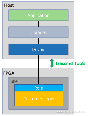
To provide an efficient and unified development and deployment platform for both accelerator vendors and users, FaaS provides both a hardware development kit (HDK) and a software development kit (SDK).

The HDK provides unified FPGA hardware APIs for all accelerator developers. With these APIs, users are free from the toughest high-speed API development and debugging tasks related to PCIe, SerDes APIs, and DDR controllers in the FPGA development process. Also, users can achieve maximum performance from the hardware platform and FPGA APIs, even if their development team lacks sufficient development capabilities or experience. Moreover, the highly efficient, reliable, unified API kit guarantees security isolation and device stability on the cloud platform. Possible API design issues of users will not cause server downtime. In addition, users are not allowed to perform unauthorized operations on hosts from the FPGA side, which safeguards the cloud security.
The HDK consists of two parts: Shell and Role. Shell is deployed in the static area and provides unified APIs. Apart from providing unified APIs and guaranteeing security and convenience, the HDK does its utmost to empower users with design flexibility through Role. Role is deployed in the dynamic area. It is pre-developed independently from Shell and can be used together with Custom Logic. Unlike Shell, Role can be replaced by users at any time to suit their needs. This combination of Shell and Role provides a lightweight Shell and balances unification, convenience, and flexibility.
The SDK also consists of two parts:
The drivers and libraries correspond to Shell and Role of the HDK, and work together with the HDK to provide users with unified and flexible software support, such as the DMA driver and register access driver.
The faascmd provides users with cloud-based FPGA management services, including security authentication, generation, download, and management of FPGA images, as well as FPGA accelerator card status query and feedback. FPGA file security is a concern when FPGA is used in a public environment. By providing keys and specifying Object Storage Service (OSS) buckets, the faascmd can effectively guarantee the privacy of users' FPGA download files. For offline development and application, users can directly download and operate on FPGA resources. However, in a cloud environment, allowing users to operate on public FPGA resources is detrimental to security. The faascmd isolates users' operation requests from physical FPGA resources. It guarantees download security while providing users with an experience similar to offline operations. It also verifies the netlists submitted by users, which enhances security and reduces risks. The faascmd also provides APIs for users to conveniently call the management tool in their apps and implement various management functions based on their accelerator features.
FaaS lowers the development difficulty for FPGA logic developers. First, ready-to-use FPGA resources on the cloud and flexible payment modes make hardware resources easily accessible. Second, FaaS simplifies the FPGA logic development process, unifies development APIs, and isolates core acceleration logic from the API debugging of peripheral hardware devices. Developers of new FPGA applications can then focus on core business acceleration logic and implement quick iteration. These are the first steps that FaaS has taken towards the popularization of FPGA resources.
Even with the simplified development process and readily available hardware resources, FPGA development is still not easy. How can we maximize the value of existing FPGA IP core and link FPGA accelerator vendors for users? One major challenge is to ensure the IP core security of FPGA acceleration at a public cloud data center, especially when we deliver and deploy IP to untrusted third parties. How does FaaS address this challenge?
The answer lies in Alibaba Cloud's FaaS IP market. Technically, Alibaba Cloud has developed the custom virtualization technology jointly with Xilinx to achieve strong isolation between IP acceleration and the deployment environment. This technology can isolate IP users from original IP netlist files. The transmission and deployment of netlist files and the whole acceleration process are invisible to users. In addition, the acceleration computing capabilities are transparently open to third-party IP users. This is another technical innovation that Alibaba Cloud has introduced in the cloud-based FPGA acceleration service. This innovation makes it impossible to pirate FPGA IPs when they are delivered on the cloud and hence provides an effective security protection mechanism.
A more stringent confidentiality mechanism is also being developed. Alibaba Cloud will soon deliver the KMS encryption service to encrypt and protect IPs. Users will need to obtain a decryption key from the KMS service each time they want to load an IP, making the IP use and download traceable. This mechanism will also ensure the security of IP advertisers' IPs at the data center. Without the KMS key assigned to an IP user, even Alibaba Cloud cannot decrypt the original netlist files.
With the help of Alibaba Cloud's FaaS IP market, even users with no FPGA development experience can obtain required acceleration logic from the IP market in one click and deploy it to their FPGA devices. Armed with ready-to-use hardware resources, unified software and hardware logic development APIs, and the IP market, Alibaba Cloud can fully deliver on its promise to the popularization of FPGA computing resources.


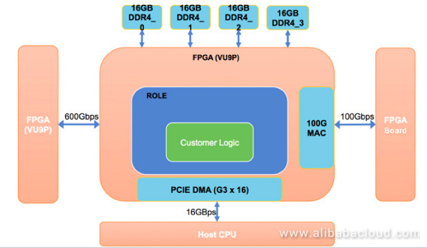
Alibaba Cloud's FaaS F3 instance uses a self-developed high-performance card as the underlying hardware. The card has dual VU9P chips on a single card. Some users might ask: Why is it designed this way? What are the merits of a single-card-dual-chip hardware design?
First, this design, along with servers developed by Alibaba Cloud, can provide a single computing instance that consists of up to 16 VU9P chips, which offers high computing density. By increasing computing density and integrating more acceleration chips into the same scale of computing unit, Alibaba Cloud can help customers effectively reduce the costs of unit computing power and increase the vertical computing power of single instances.
The dual VU9P chips on a single card access the system through PCIe. But how do the two chips communicate with each other? Must they communicate only through the PCIe bus? No. Apart from the FPGA Direct capability, which uses PCIe for communication, the card has a special design. The two chips are interconnected through a high-speed channel, allowing two FPGAs to communicate at a rate of up to 600 Gbit/s. This technology is called FPGA Link. To understand the significance of this, you need to know that the optical port of mainstream access switches deployed at a data center supports a maximum communication rate only of 100 Gbit/s. The switches with a higher rate of 200 Gbit/s are still in trial deployment.
Just think about it: With no extra switches or optical port hardware, two FPGA chips can communicate with each other with an extremely low delay at a rate six times that of mainstream optical ports. This allows users to launch a large number of new FPGA acceleration applications at very low cost. For example, in scenarios where small-scale chip simulation requires two devices, the whole simulation module can be split and deployed to two chips, which then interconnect through a high-speed channel to exchange data and signals. In other scenarios, functional modules may need to be deployed to two FPGA chips that exchange a great amount of data. For example, in a video transcoding scenario, the small-sized decoding and video processing units with many modules involved are deployed to one FPGA chip while the encoding unit that occupies a large area is deployed to the other FPGA chip. The encoding and decoding units exchange raw video streams through the high-speed channel. This can make deployment considerably easier, decouple the dependency between two modules, and reduce design complexity. You can also think of other scenarios that require streamline processing and massive data exchange. It is in such scenarios that the dual chips of Alibaba Cloud's F3 instance deliver the maximum value to customers.
Some application scenarios still require on-card DDR storage. Alibaba Cloud's F3 instance provides 64 GB customer-available DDR memory for each FPGA. The 64 GB DDR memory can be divided into four channels that respectively connect to the three silicon units on the VU9P. The 16 GB DDR memory provided by one channel remains in use while the 48 GB DDR memory provided by the other three channels is loaded and optionally used by Custom Logic.
In addition to the FPGA Direct and 600 Gbit/s FPGA Link capabilities, the dual-chip instance card can interconnect with other duel-chip instance cards through 400 Gbit/s optical ports. The 400 Gbit/s Ethernet driver is accelerated by the MAC hard core built in by Xilinx, which does not occupy any logical area. By using Ethernet or a custom lightweight communication protocol, we can establish a two-dimensional mesh or ring connection among the 16 or more chips. In doing so, we can create more usage patterns and application scenarios for inter-chip connection.
We provide a figure for you to have a visual concept about the above mentioned hardware technology.
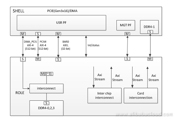
The following figure shows the F3 logic structure.
Shell is the static area of an FPGA and includes the user PCIe, management PCIe, card management system, and a DDR access channel. For the sake of card security and stability, users are not authorized to modify the Shell area.
The concept of Role is put forward during the design. The encapsulation of Role is similar to that of Shell. Role and Custom Logic are deployed in the dynamic area. With the use of Role, a more lightweight Shell can be implemented. Role allows a single Shell to support both OpenCL and RTL development. The abstraction of Role also makes FPGA development easier. We provide the basic Role and allow users to customize their own Role. We expect more third-party designers to share their Role design to make FaaS a more fascinating platform.
Interconnect: Provides four DDR channels for users and USER_PCIe to access. This module helps users isolate clock domains and allows users to access four DDR channels in the same clock domain.
Inter chip interconnect: Provides an interconnection path between the dual chips on a single FPGA card.
Card interconnect: Provides an interconnection path between FPGA cards.
Custom Logic: User-defined logic. Custom Logic is a part of Role and belongs to the dynamic loading area. To allow users to define Custom Logic in a standardized way, we use the AXI-4 and AXI-LITE APIs in the RTL design.
Best Practice on Testing System Event Processing Program for ECS Instances

33 posts | 12 followers
FollowJDP - July 30, 2021
Alibaba Clouder - September 29, 2017
AlibabaCloud_Network - April 19, 2019
Alibaba Cloud TC Content - November 22, 2021
Data Geek - April 29, 2024
JJ Lim - April 19, 2023

33 posts | 12 followers
Follow ECS(Elastic Compute Service)
Elastic and secure virtual cloud servers to cater all your cloud hosting needs.
Learn More Elastic High Performance Computing Solution
High Performance Computing (HPC) and AI technology helps scientific research institutions to perform viral gene sequencing, conduct new drug research and development, and shorten the research and development cycle.
Learn More Elastic High Performance Computing
A HPCaaS cloud platform providing an all-in-one high-performance public computing service
Learn More Container Compute Service (ACS)
A cloud computing service that provides container compute resources that comply with the container specifications of Kubernetes
Learn MoreMore Posts by Alibaba Cloud ECS
5761785765702174 April 1, 2021 at 12:54 pm
what about price / costs for fpga / network / storage?any hidden fees? any limitation on network throughput?